- 您现在的位置:买卖IC网 > Sheet目录344 > MSC8126ADSE (Freescale Semiconductor)KIT ADVANCED DEV SYSTEM 8126
Electrical Characteristics
2.5.4.3
Reset Timing Tables
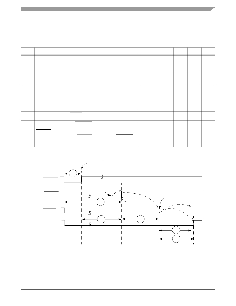
Table 12 and Figure 9 describe the reset timing for a reset configuration write through the direct slave interface (DSI) or
through the system bus.
Table 12. Timing for a Reset Configuration Write through the DSI or System Bus
No.
Characteristics
Expression
Min
Max
Unit
1
Required external PORESET duration minimum
16/CLKIN
2
? CLKIN = 20 MHz
? CLKIN = 133 MHz (400 MHz core)
? CLKIN = 166 MHz (500 MHz core)
Delay from deassertion of external PORESET to deassertion of internal
1024/CLKIN
800
120
96
800
—
—
ns
ns
ns
PORESET
3
? CLKIN = 20 MHz to 166 MHz
Delay from de-assertion of internal PORESET to SPLL lock
6400/(CLKIN/RDF)
6.17
51.2
μs
? CLKIN = 20 MHz (RDF = 1)
? CLKIN = 133 MHz (RDF = 2) (400 MHz core)
? CLKIN = 166 MHz (RDF = 2) (500 MHz core)
(PLL reference
clock-division factor)
320
96
77
320
96
77
μs
μs
μs
5
Delay from SPLL to HRESET deassertion
6
? REFCLK = 40 MHz to 166 MHz
Delay from SPLL lock to SRESET deassertion
? REFCLK = 40 MHz to 166 MHz
512/REFCLK
515/REFCLK
3.08
3.10
12.8
12.88
μs
μs
7
Setup time from assertion of RSTCONF , CNFGS, DSISYNC, DSI64,
3
—
ns
CHIP_ID[0–3], BM[0–2], SWTE, and MODCK[1–2] before deassertion of
PORESET
8
Hold time from deassertion of PORESET to deassertion of RSTCONF ,
5
—
ns
CNFGS, DSISYNC, DSI64, CHIP_ID[0–3], BM[0–2], SWTE, and
MODCK[1–2]
Note:
Timings are not tested, but are guaranteed by design.
RSTCONF, CNFGS, DSISYNC, DSI64
CHIP_ID[0–3], BM[0–2], SWTE, MODCK[1–2]
PORESET
Input
PORESET
Internal
1
pins are sampled
Host programs
Reset Configuration
Word
SPLL is locked
HRESET
Output (I/O)
SRESET
1+2
2
MODCK[3–5]
3
(no external indication)
Output (I/O)
Reset configuration write
sequence during this
period.
SPLL
locking period
5
6
Figure 9. Timing Diagram for a Reset Configuration Write
MSC8126 Quad Digital Signal Processor Data Sheet, Rev. 15
Freescale Semiconductor
21
发布紧急采购,3分钟左右您将得到回复。
相关PDF资料
MSC8144ADS
ADS FOR MSC8144 DEVICE
MSC8156EVM
EVAL MODULE FOR MSC8156 LC
MSL1060AW
IC LED DRIVER 6 STRING
MSL1061AV
IC LED DRIVER 6 STRING
MSL2041GU
IC LED DRIVER 4 STRING
MSL2100BR
IC LED DRIVER 8 STRING
MSL2160DQ
IC LED DRIVER 16 STRING
MSL2162DQ
IC LED DRIVER 16 STRING
相关代理商/技术参数
MSC8126MP8000
功能描述:DSP 16BIT 500MHZ MULTI 431FCPBGA RoHS:否 类别:集成电路 (IC) >> 嵌入式 - DSP(数字式信号处理器) 系列:StarCore 标准包装:40 系列:TMS320DM64x, DaVinci™ 类型:定点 接口:I²C,McASP,McBSP 时钟速率:400MHz 非易失内存:外部 芯片上RAM:160kB 电压 - 输入/输出:3.30V 电压 - 核心:1.20V 工作温度:0°C ~ 90°C 安装类型:表面贴装 封装/外壳:548-BBGA,FCBGA 供应商设备封装:548-FCBGA(27x27) 包装:托盘 配用:TMDSDMK642-0E-ND - DEVELPER KIT W/NTSC CAMERA296-23038-ND - DSP STARTER KIT FOR TMS320C6416296-23059-ND - FLASHBURN PORTING KIT296-23058-ND - EVAL MODULE FOR DM642TMDSDMK642-ND - DEVELOPER KIT W/NTSC CAMERA
MSC8126TMP6400
功能描述:DSP 16BIT 400MHZ MULTI 431FCPBGA RoHS:否 类别:集成电路 (IC) >> 嵌入式 - DSP(数字式信号处理器) 系列:StarCore 标准包装:2 系列:StarCore 类型:SC140 内核 接口:DSI,以太网,RS-232 时钟速率:400MHz 非易失内存:外部 芯片上RAM:1.436MB 电压 - 输入/输出:3.30V 电压 - 核心:1.20V 工作温度:-40°C ~ 105°C 安装类型:表面贴装 封装/外壳:431-BFBGA,FCBGA 供应商设备封装:431-FCPBGA(20x20) 包装:托盘
MSC8126TVT6400
功能描述:IC DSP QUAD 16B 400MHZ 431FCPBGA RoHS:是 类别:集成电路 (IC) >> 嵌入式 - DSP(数字式信号处理器) 系列:StarCore 标准包装:2 系列:StarCore 类型:SC140 内核 接口:DSI,以太网,RS-232 时钟速率:400MHz 非易失内存:外部 芯片上RAM:1.436MB 电压 - 输入/输出:3.30V 电压 - 核心:1.20V 工作温度:-40°C ~ 105°C 安装类型:表面贴装 封装/外壳:431-BFBGA,FCBGA 供应商设备封装:431-FCPBGA(20x20) 包装:托盘
MSC8126VT8000
功能描述:IC DSP QUAD 16B 500MHZ 431FCPBGA RoHS:是 类别:集成电路 (IC) >> 嵌入式 - DSP(数字式信号处理器) 系列:StarCore 标准包装:2 系列:StarCore 类型:SC140 内核 接口:DSI,以太网,RS-232 时钟速率:400MHz 非易失内存:外部 芯片上RAM:1.436MB 电压 - 输入/输出:3.30V 电压 - 核心:1.20V 工作温度:-40°C ~ 105°C 安装类型:表面贴装 封装/外壳:431-BFBGA,FCBGA 供应商设备封装:431-FCPBGA(20x20) 包装:托盘
MSC81325M
制造商:STMICROELECTRONICS 制造商全称:STMicroelectronics 功能描述:RF & MICROWAVE TRANSISTORS AVIONICS APPLICATIONS
MSC81350M
制造商:STMICROELECTRONICS 制造商全称:STMicroelectronics 功能描述:RF & MICROWAVE TRANSISTORS AVIONICS APPLICATIONS
MSC81400M
制造商:STMICROELECTRONICS 制造商全称:STMicroelectronics 功能描述:RF & MICROWAVE TRANSISTORS AVIONICS APPLICATIONS
MSC81402
制造商:STMICROELECTRONICS 制造商全称:STMicroelectronics 功能描述:RF & MICROWAVE TRANSISTORS GENERAL PURPOSE AMPLIFIERS APPLICATIONS
